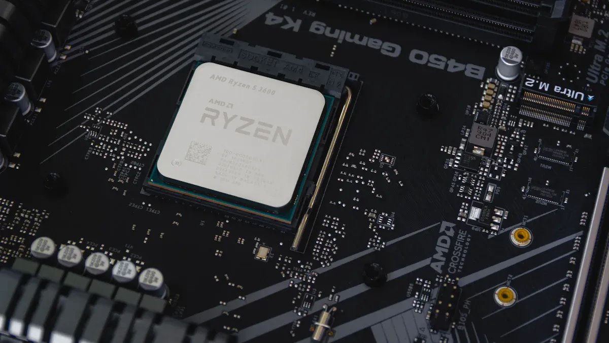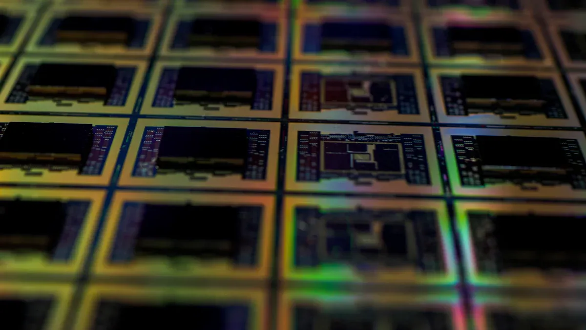
Epitaxy refers to the process of depositing thin crystalline layers on a substrate, utilizing the substrate’s structure to guide the crystallinity and orientation of the growth. This technique creates a flawless crystalline foundation for semiconductor devices by forming a single crystal layer, typically between 0.5 and 20 microns thick. The epitaxial growth process is crucial for enabling efficient electron transmission, which is essential for high-performance devices.
The global epi wafer market reflects this importance, with projections showing its value rising from USD 3,997.8 million in 2025 to USD 9,347.1 million by 2032, at a CAGR of 12.9%. Additionally, the epi semiconductor industry benefits from equipment innovations, which are growing at a CAGR of 10% due to increasing demand in telecommunications and automotive sectors. These trends underscore the significance of epi quality in advancing semiconductor technologies.
المداخل الرئيسية
- Epitaxy helps make strong crystal layers in semiconductors. This improves how devices work and makes them last longer.
- There are two types of epitaxy: homoepitaxy and heteroepitaxy. These allow using different materials and creating new device designs.
- Chemical Vapor Deposition (CVD) is an important epitaxy method. It controls layer thickness and material mix for advanced uses.
- Doping in epitaxy changes how materials conduct electricity. This helps create special semiconductor devices.
- Epitaxy helps build technologies like 5G and AI. It increases the need for better parts in modern electronics.
Understanding Epitaxy in Semiconductor Fabrication

Definition and Purpose
Epitaxy involves the growth of a crystalline layer on a substrate, where the substrate’s atomic arrangement determines the structure and orientation of the new layer. This process ensures the creation of a high-quality single crystal layer, which is essential for manufacturing advanced semiconductor devices. The epitaxial layer provides a controlled environment for electron movement, enhancing the performance and reliability of electronic components. By enabling precise control over material properties, epitaxy plays a critical role in the development of modern technologies.
Types: Homoepitaxy and Heteroepitaxy
Epitaxy can be classified into two main types based on the relationship between the substrate and the grown layer:
- Homoepitaxy: This type involves the deposition of a crystalline layer that matches the substrate’s material. For example, growing silicon on a silicon substrate ensures uniformity and compatibility. Homoepitaxy is commonly used in applications requiring high purity and minimal defects.
- Heteroepitaxy: In this type, the grown layer differs from the substrate material. For instance, gallium arsenide (GaAs) can be deposited on a silicon substrate. Heteroepitaxy enables the integration of materials with distinct properties, expanding the possibilities for innovative device designs.
Both types of epitaxy contribute to advancements in semiconductor technology by offering flexibility in material selection and design.
Applications in Semiconductor Devices
Epitaxy serves as a foundation for numerous semiconductor devices, enabling their efficient operation and enhanced performance. Some key applications include:
- Transistors: Epitaxial layers improve the electrical properties of transistors, which are essential components in integrated circuits.
- LEDs and Lasers: The process allows for the precise growth of materials like gallium nitride (GaN), which is crucial for light-emitting diodes (LEDs) and laser diodes.
- Power Electronics: Epitaxy enhances the efficiency and reliability of power devices, such as silicon carbide (SiC) and gallium nitride (GaN) transistors, used in electric vehicles and renewable energy systems.
The Asia-Pacific region leads the market for epitaxial wafers, driven by demand in emerging economies like China and India. Telecommunications, particularly the deployment of 5G networks, dominates the market due to the need for high-speed data transmission. The global market for epitaxial wafers is projected to exceed $1 billion by 2025, fueled by the increasing demand for high-performance electronic devices and the adoption of new materials and technologies.
Technical Aspects of the Epitaxy Process
Chemical Vapor Deposition (CVD) Method
Chemical Vapor Deposition (CVD) is a widely used method for epitaxial growth. This process involves the chemical reaction of gaseous precursors on a heated substrate, resulting in the deposition of a thin crystalline layer. The substrate temperature plays a critical role in ensuring proper chemical reactions and uniform layer growth.
CVD offers several advantages, including precise control over layer thickness and composition. It also enables the deposition of high-purity materials, which is essential for advanced semiconductor devices. Variants of CVD, such as low-pressure CVD (LPCVD) and metal-organic CVD (MOCVD), cater to specific applications, such as the growth of silicon or compound semiconductors like gallium nitride (GaN).
Equipment: Reactors, Susceptors, and Substrates
The epitaxy process relies on specialized equipment to achieve high-quality results. Reactors serve as the primary chambers where the epitaxial growth occurs. These reactors maintain controlled environments, including temperature, pressure, and gas flow, to ensure uniform deposition.
Susceptors, typically made of materials like graphite or silicon carbide, hold the substrate during the process. They absorb heat efficiently, ensuring the substrate reaches the desired temperature for epitaxial growth. Substrates, on the other hand, act as the foundation for the crystalline layer. Their material and surface quality significantly influence the outcome of the epitaxy process.
The integration of advanced equipment has enhanced the efficiency and precision of the epi semiconductor fabrication process, meeting the growing demand for high-performance devices.
Role of Doping in Epitaxy
Doping introduces impurities into the epitaxial layer to modify its electrical and structural properties. This technique allows manufacturers to tailor the material’s characteristics, such as conductivity and bandgap, to suit specific applications.
Different doping elements produce distinct effects on the epitaxial layer. For instance, magnesium (Mg) widens the bandgap, while lithium (Li) and iron (Fe) narrow it. These changes influence the material’s electrical conductivity, enabling the creation of devices with unique functionalities.
| Doping Element | Effect on Band Gap | Effect on Electrical Conductivity |
|---|---|---|
| Mg | Widening | Modifies properties |
| Li | Narrowing | Modifies properties |
| Fe | Narrowing | Modifies properties |
The concentration of doping elements also affects the material’s magnetization. By adjusting the doping concentration, manufacturers can achieve tunable magnetic properties, which are crucial for specific applications.
| Doping Concentration | Effect on Magnetization |
|---|---|
| Variable | Tunable |
Doping plays a pivotal role in the epi semiconductor industry by enabling the production of materials with customized properties. This capability supports the development of innovative devices for emerging technologies.
Techniques Used in Epitaxy

Vapor Phase Epitaxy (VPE)
Vapor Phase Epitaxy (VPE) is a widely adopted technique for growing epitaxial layers. It involves the reaction of gaseous precursors on a heated substrate, forming a thin crystalline layer. This method offers precise control over the thickness and composition of the layer. VPE is particularly effective for producing high-purity materials, making it suitable for advanced semiconductor applications.
A comparison of epitaxy techniques highlights the advantages of VPE. For instance, second-generation (Gen II) substrates used in VPE show no yield issues with larger contact areas. They also exhibit better breakdown voltage and minimal leakage current compared to first-generation (Gen I) substrates.
| Epitaxy Technique | Yield Impact | Breakdown Voltage | Leakage Current |
|---|---|---|---|
| Gen I Substrates | Loss of yield with larger areas | Observed issues | Increased leakage |
| Gen II Substrates | No yield issues | Better performance | Minimal leakage increase |
Molecular Beam Epitaxy (MBE)
Molecular Beam Epitaxy (MBE) is a highly controlled process that uses molecular or atomic beams to deposit thin films on a substrate. This technique operates in an ultra-high vacuum environment, ensuring exceptional purity and precision. MBE is ideal for research and development due to its ability to create complex structures with atomic-level accuracy.
MBE’s precision allows for the fabrication of devices with unique properties. It is often used to develop materials for quantum computing and optoelectronics. However, its slower growth rate makes it less suitable for large-scale production.
Liquid Phase Epitaxy (LPE)
Liquid Phase Epitaxy (LPE) involves the deposition of a crystalline layer from a liquid phase. This method is cost-effective and efficient for producing thick layers. LPE is commonly used for fabricating optoelectronic devices, such as LEDs and laser diodes.
Although LPE is less precise than VPE or MBE, it remains a valuable technique for applications requiring thicker layers. Its simplicity and low cost make it an attractive option for specific industrial applications.
Ensuring Quality in Epitaxy
Impact of Defects on Semiconductor Performance
Defects in epitaxial layers can significantly affect the performance of semiconductor devices. These imperfections disrupt the crystalline structure, leading to issues such as reduced electron mobility and increased power loss. Manufacturers must monitor defect rates closely to ensure optimal device functionality.
The following table highlights how specific defect rates influence semiconductor performance metrics:
| القياس | Description |
|---|---|
| Positive Predictive Value (PPV) | Indicates the likelihood that a reported faulty chip is genuinely defective. |
| Faulty Street Ratio >0.5% | Reliable fault detection with less than 10% flawless chips, enabling automated analysis. |
| Faulty Street Ratio >0.2% | Fault detection accuracy ranges from 10% to 50%, requiring semi-automatic quantification. |
| Faulty Street Ratio <0.2% | Demands a recall/specificity above 99.5% for reliable quality assessment. |
By addressing these defect rates, manufacturers can enhance the reliability and efficiency of epi semiconductor devices.
Methods for High-Quality Epitaxial Layers
Achieving high-quality epitaxial layers requires advanced cleaning and treatment methods. These processes remove contaminants and ensure a pristine substrate surface for crystal growth.
- Reactive hydrogen plasma cleaning effectively eliminates polymer residues from materials like WS2, ensuring superior layer quality.
- Conventional wet cleaning methods often fail to remove residues and may damage the films.
- Photoluminescence measurements confirm that dry cleaning methods, such as hydrogen plasma exposure, do not introduce additional damage.
These techniques demonstrate the importance of adopting innovative cleaning methods to maintain the integrity of epitaxial layers.
Importance of Metrology and Inspection
Metrology and inspection play a vital role in ensuring the quality of epitaxial layers. Advanced techniques provide precise measurements of layer thickness, composition, and relaxation.
| التقنية | الاستحقاقات الرئيسية | التطبيق |
|---|---|---|
| HRXRD | High accuracy in measuring thickness and composition | Process control for SiGe layers |
| XRR | Excellent repeatability in determining relaxation | In-line monitoring of epitaxial films |
These tools enable manufacturers to maintain stringent quality standards, ensuring the production of high-performance devices.
Epitaxy’s Role in Advancing Semiconductor Technology
Contribution to Miniaturization and Performance
Epitaxy plays a pivotal role in the miniaturization of semiconductor devices while enhancing their performance. The demand for high-performance devices has driven significant growth in the epitaxy equipment market. Manufacturers are investing heavily in research and development to improve process control, efficiency, and material compatibility. These advancements enable the production of smaller, more efficient devices that meet the needs of modern applications.
- The epitaxy equipment market is expanding rapidly due to the increasing demand for advanced semiconductor devices.
- Technological innovations and R&D investments are key drivers of this growth, supporting miniaturization and performance improvements.
- Enhanced process control and material compatibility in epitaxy equipment stimulate market growth and innovation.
The evolving landscape of the epitaxy market highlights its importance in creating compact, high-performance devices. This trend aligns with the growing need for integration in consumer electronics and other industries.
Importance in Emerging Technologies like 5G and AI
Epitaxy is essential for enabling cutting-edge technologies such as 5G and artificial intelligence (AI). The epitaxial wafer market has grown significantly due to the demand for high-performance components in these applications. Epitaxial wafers are integral to modern electronics, including integrated circuits and light-emitting diodes. These components form the backbone of 5G and AI technologies.
The shift toward wide bandgap materials, such as silicon carbide and gallium nitride, has further enhanced the performance of devices used in electric vehicles and renewable energy systems. These materials, enabled by epitaxy, provide the efficiency and reliability required for next-generation technologies.
Future Trends in Epi Semiconductor Fabrication
The future of epi semiconductor fabrication is shaped by rapid innovation and evolving market demands. Advancements in silicon carbide epitaxial reactors and process automation are driving efficiency and sustainability in semiconductor manufacturing.
| Insight Type | Description |
|---|---|
| Innovation Trends | Rapid innovation in SiC epitaxial reactors driven by technology advancements and market needs. |
| Advanced Epitaxy Methods | Integration of advanced methods and automation to enhance efficiency and sustainability. |
| Industry Deployment | Growth in sectors like aerospace, automotive, and power electronics reflects market potential. |
| Sustainability Measures | Emphasis on sustainability influences technology adoption in semiconductor fabrication. |
The competitive environment fosters innovation and investment, ensuring the continuous evolution of epitaxy technologies. These advancements will support the development of more efficient and sustainable semiconductor devices, meeting the demands of emerging industries.
Epitaxy plays a vital role in semiconductor fabrication by enabling the growth of high-quality crystalline layers. This process enhances device performance through precise control of doping concentrations and improved electrical characteristics, such as higher disintegration voltage and lower collector resistance. Techniques like chemical vapor deposition ensure the creation of reliable semiconductor layers for advanced applications.
- Epitaxy supports the development of high-performance devices, including transistors and power electronics.
- Ongoing advancements in epitaxial methods drive innovation in emerging technologies like 5G and AI.
These contributions position epitaxy as a cornerstone of future semiconductor innovations.
FAQ
What is the main purpose of epitaxy in semiconductor fabrication?
Epitaxy creates a high-quality crystalline layer on a substrate. This layer provides a controlled environment for electron movement, improving the performance and reliability of semiconductor devices.
How does homoepitaxy differ from heteroepitaxy?
Homoepitaxy grows a layer of the same material as the substrate, ensuring uniformity. Heteroepitaxy uses a different material, enabling unique properties for advanced device designs.
Why is doping important in the epitaxy process?
Doping modifies the electrical properties of the epitaxial layer. It allows manufacturers to tailor conductivity and other characteristics, supporting the creation of specialized semiconductor devices.
What role does Chemical Vapor Deposition (CVD) play in epitaxy?
CVD deposits thin crystalline layers by reacting gaseous precursors on a heated substrate. This method ensures precise control over layer thickness and composition, essential for high-performance devices.
How does epitaxy contribute to emerging technologies like 5G and AI?
Epitaxy enables the production of high-performance components, such as transistors and LEDs. These components are critical for the speed and efficiency required in 5G networks and AI applications.


